Product Features
● Supports 1.25Gbps/1.0625Gbps bit rates ● Duplex LC connector ● Hot pluggable SFP footprint ● 850nm VSCEL laser transmitter and PIN photo-detector ● Applicable for 550m on 50/125µm, 300m on 62.5/125µm MMF connection ● Low power consumption, < 0.8W ● Digital Diagnostic Monitor Interface ● Compliant with SFP MSA and SFF-8472 ● Very low EMI and excellent ESD protection ● Operating case temperature: Commerical:0 to 70 °C Industrial:-40 to 85 °CPin Definitions And Functions
Absolute Maximum Ratings
| Parameter | Symbol | Min. | Max. | Unit | Note |
| Supply Voltage | Vcc | -0.5 | 4.0 | V | |
| Storage Temperature | TS | -40 | 85 | °C | |
| Relative Humidity | RH | 0 | 85 | % |
Applications
● Gigabit Ethernet ● Fiber Channel ● Switch to Switch interface ● Switched backplane applications ● Router/Server interface ● Other optical transmission systemsGeneral Operating Characteristics
| Parameter | Symbol | Min. | Typ | Max. | Unit | Note |
| Data Rate | DR | 1.25 | Gb/s | |||
| Supply Voltage | Vcc | 3.13 | 3.3 | 3.47 | V | |
| Supply Current | Icc5 | 220 | mA | |||
| Operating Case Temp. | Tc | 0 | 70 | °C | ||
| TI | -40 | 85 |
Electrical Characteristics (TOP(C) = 0 to 70 ℃, TOP(I) =-40 to 85 ℃,VCC = 3.13 to 3.47 V)/h2>
| Parameter | Symbol | Min. | Typ | Max. | Unit | Note | |
| Transmitter | |||||||
| Differential data input swing | VIN,PP | 250 | 1200 | mVpp | 1 | ||
| Tx Disable Input-High | VIH | 2.0 | Vcc+0.3 | V | |||
| Tx Disable Input-Low | VIL | 0 | 0.8 | V | |||
| Tx Fault Output-High | VOH | 2.0 | Vcc+0.3 | V | 2 | ||
| Tx Fault Output-Low | VOL | 0 | 0.8 | V | 2 | ||
| Input differential impedance | Rin | 100 | Ω | ||||
| Receiver | |||||||
| Differential data output swing | Vout,pp | 250 | 550 | mVpp | 3 | ||
| Rx LOS Output-High | VROH | 2.0 | Vcc+0.3 | V | 2 | ||
| Rx LOS Output-Low | VROL | 0 | 0.8 | V | 2 | ||
Optical Characteristics (TOP(C) = 0 to 70 ℃, TOP(I) =-40 to 85 ℃,VCC = 3.13 to 3.47 V)
| Parameter | Symbol | Min. | Typ | Max. | Unit | Note |
| Transmitter | ||||||
| Operating Wavelength | λ | 840 | 850 | 860 | nm | |
| Ave. output power (Enabled) | PAVE | -9 | 0 | dBm | 1 | |
| Extinction Ratio | ER | 9 | dB | 1 | ||
| RMS spectral width | Δλ | 0.65 | nm | |||
| Rise/Fall time (20%~80%) | Tr/Tf | 0.25 | ps | 2 | ||
| Output Optical Eye | Compliant with IEEE802.3 z &ITU G.957 Compliant (class 1 aser safety) | |||||
| Receiver | ||||||
| Operating Wavelength | λ | 840 | 850 | 860 | nm | |
| Receiver Sensitivity | PSEN1 | -18 | dBm | 3 | ||
| Overload | PAVE | -3 | dBm | 3 | ||
| LOS Assert | Pa | -35 | dBm | |||
| LOS De-assert | Pd | -20 | dBm | |||
| LOS Hysteresis | Pd-Pa | 0.5 | dB | |||
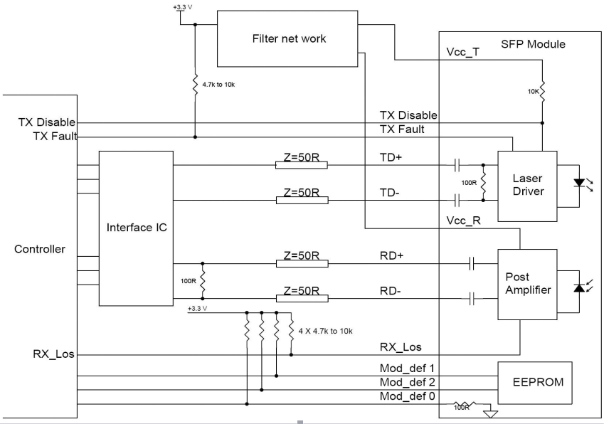
Typical Interface Circuit
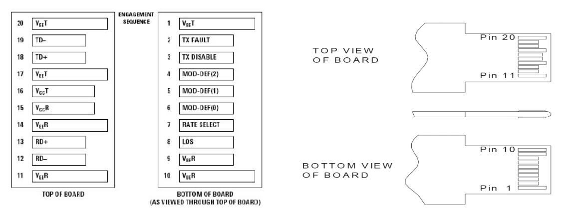
| Pin | Symbol | Name/Description | Notes |
| 1 | VeeT | Tx ground | |
| 2 | Tx Fault | Tx fault indication, Open Collector Output, active “H” | 1 |
| 3 | Tx Disable | LVTTL Input, internal pull-up, Tx disabled on “H” | 2 |
| 4 | MOD-DEF2 | 2 wire serial interface data input/output (SDA) | 3 |
| 5 | MOD-DEF1 | 2 wire serial interface clock input (SCL) | 3 |
| 6 | MOD-DEF0 | Model present indication | 3 |
| 7 | Rate select | No connection | |
| 8 | LOS | Rx loss of signal, Open Collector Output, active “H” | 4 |
| 9 | VeeR | Rx ground | |
| 10 | VeeR | Rx ground | |
| 11 | VeeR | Rx ground | |
| 12 | RD- | Inverse received data out | 5 |
| 13 | RD+ | Received data out | 5 |
| 14 | VeeR | Rx ground | |
| 15 | VccR | Rx power supply | |
| 16 | VccT | Tx power supply | |
| 17 | VeeT | Tx ground | |
| 18 | TD+ | Transmit data in | 6 |
| 19 | TD- | Inverse transmit data in | 6 |
| 20 | VeeT | Tx ground |
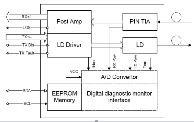
Functional Diagram
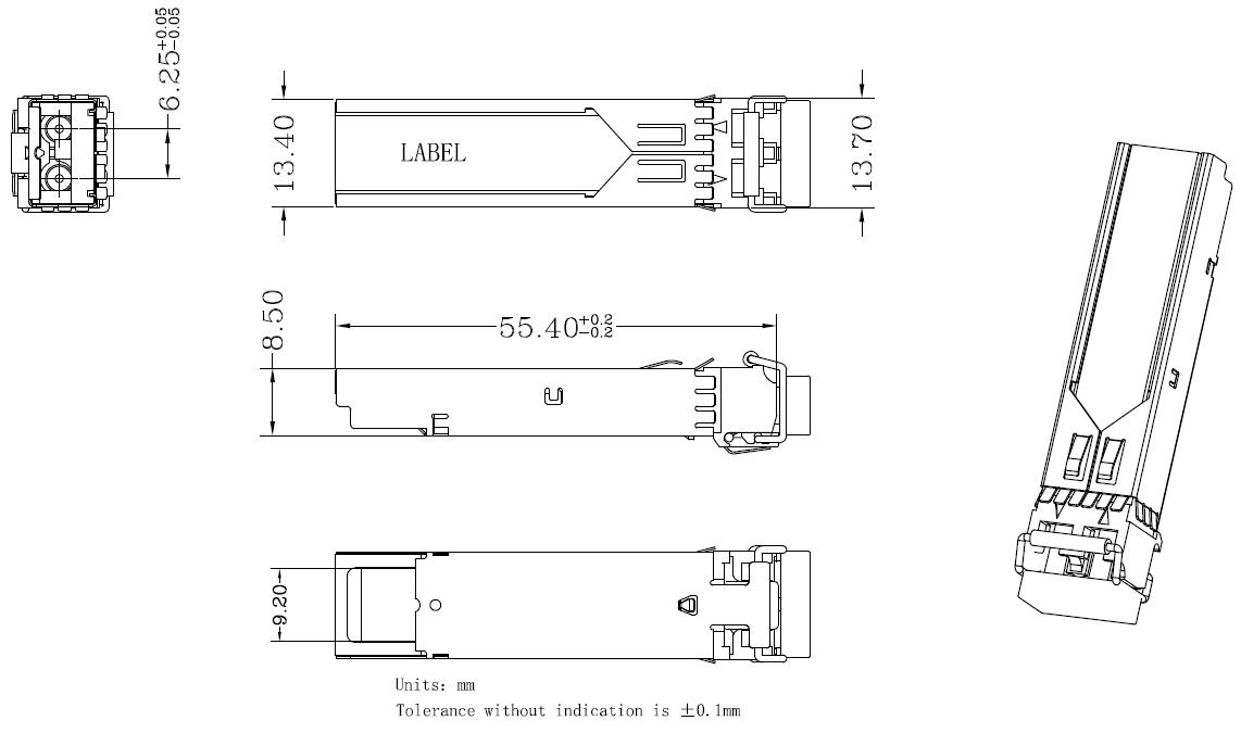
Package Dimensions